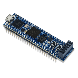
Xilinx Artix-7 FPGA design using block ram, XADC, PLL and a SPI slave (SCARF). The block ram is dual port and can be written by either SPI or XADC samples, and only read by SPI. The PLL (250MHz output) was created by the Clock Wizard and the XADC by the XADC Wizard in Vivado. The block ram is 64k bytes in size and can capture 65536 samples from the XADC (upper 8bits of the 12bit values). I use Python to have a Raspberry Pi perform various SPI bus cycles to my CMOD A7 FPGA board. The XADC converts an input voltage between 0 to 3.3V.
The block ram is initialized with non-zero hex values from the bram_initial_hex_values.data file.
This is a proof of concept, as I wanted to make a project that (1) used block ram resources initialized from a file, (2) use the XADC resource, (3) use a PLL resource and (4) read XADC values & read/write block ram using SPI
